|
Intel 810 Chipset Review Reviewed by Vijay Anand (8/6/99) <Introduction><The i810><The
GMCH><The ICH> Introduction** All benchmakrs, results and opinions are based on the world's
1st i810 motherboard, the DFI-PW65D, which I had for testing. But generally, most i810
boards should have many similarities between them, hence this article should be valid for
all i810 motherboards** The i810 ArchitectureTraditionally everything on the system communicates with the CPU and
memory via the slow and maybe saturated central PCI bus but with the introduction of the
i810 chipset, a new architecture is born and is called the Accelerated Bus Architecture
(AHA). AHA allows direct communication of the CPU, memory, graphics (built-in to the
chipset) and other peripherals. It replaces the PCI as the central bus and the typical
North and South-bridge chipsets with a three-hub architecture. The three hubs (separate
chips) are the Graphics and Memory Controller Hub (GMCH), the I/O Controller Hub (ICH) and
the Firmware Hub (FWH). The below diagram will help to explain how the new AHA works and
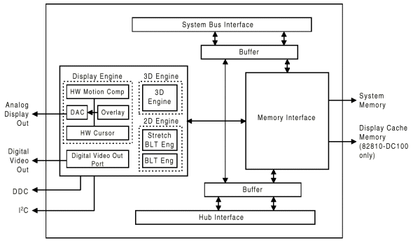
how each hub helps: The GMCHThe GMCH as the name suggests contains the graphics and memory controllers and the following is the proper break down of components: |


System Bus Interface
System Memory Interface
Display Interface
Display Cache Interface ( 82810-DC100 only)
Digital TV-Out
Clock Signals
Miscellaneous Interface Signals
Hub Interface
There are 2 versions of the GMCH, the 82810 GMCH and the 82810-DC100 GMCH, the main difference being that the DC100 version has the Display Cache Interface integrated which supports 4mb of external display cache. Both versions of the GMCH are pin-compatible, hence one manufacturer can have a low cost model and the premium model without the need to re-design the base model. Here's a schematic of the GMCH:
The graphics part is handled by an integrated i752 core basically a spruced up i740. It's key features are that it has dual-rendering pipes, motion-compensation for DVD, 1600x1200 desktop resolution, 230Mhz RAMDAC, a maximum of 16-bit colour support in 3D and a Direct-AGP connection that is essentially a direct access to the system memory to store all graphics data as the GMCH itself has no local memory. And guess what? The memory bus is locked at 100mhz, while the FSB can be 66/100Mhz (the official ones but there are the usual unofficial ones by the manufacturers! ). This means even if you intend to overclock the system by changing the FSB, the memory-bus is still at 100mhz, hence any standard PC100 rams will do the job without you needing to hunt for those faster and expensive rams. But you can't use your older PC-66 rams unless they do happen to be of good quality and are happy to run at 100Mhz. Now back to the Direct-AGP connection, since the graphics controller (in the GMCH) has a direct connection to the memory, the bandwidth is 800mb/s (64-bit memory bus / 8-bits x 100mhz) and that is more than AGP 2X transfers of 533mb/s (32-bit / 8-bits x 133Mhz)!! Don't get excited yet because all the graphics adapters have their own local memory that has far higher bandwidth between the graphics chipset and the on-board memory but once the graphics data (e.g. textures) are too big for the local memory, they'll have to be stored in the system's memory if the graphics adapter uses an AGP connection. In that situation, the GMCH's integrated video becomes more favourable because of it's higher bandwidth to the system's memory but this isn't good enough as the video engine itself isn't as powerful as what Intel is marketing it as (would you believe TNT-like performance for an i752 ?! ).
Fortunately, the costlier version of the GMCH called the i82810-DC100 can support an optional 4mb of cache for the integrated video (the cheaper i82810 GMCH can't support the extra cache). The DC100 just means that it uses 100Mhz cache. There is a possibility of a DC133 because the BIOS supports the setting of the cache speed either to 100 or 133. The odd thing is that that there is a separate bus from the GMCH to the cache but it's only 32-bits wide, meaning only a 400mb/s bandwidth!! Makes any sense? Well at least the cache is given to the integrated video to lessen the system memory's burden. Overall the idea of this and the Direct-AGP connection is far better than the old UMA-architecture in older motherboard designs. Oh and I forgot to tell you that 1mb of your system memory is reserved from the second you switch on the PC as a display frame buffer. Once in windows, it will use the Intel Dynamic Video Memory Technology (D.V.M.) technology to freely allocate itself an amount of system memory as and when it needs to. Here's a snippet from Intel:
"The internal graphics device on both the 82810 and 82810-DC100 support Intel Dynamic Video Memory Technology (D.V.M.). With D.V.M, the allocated size of system memory used for display graphics can be dynamically altered. For example, if 2 MB of system memory is needed, the driver allocates this amount. If later, only 1.5 MB is needed, the driver allocates the 1.5-MB size freeing up the remaining 512 KB for system use.
In addition to D.V.M., the 82810-DC100 supports Display Cache (DC). The graphics engine of the 82810-DC100 uses DC for implementing rendering buffers (e.g., Z buffers). This rendering model requires 4 MB of display cache and allows graphics rendering (performed across the graphics display cache bus) and texture MIP map access (performed across the system memory bus) simultaneously. Using D.V.M. all graphics rendering is implemented in system memory. The system memory bus is arbitrated between texture MIP-map accesses and rendering functions."
This kind of video-integrated solution can use some Megabytes of your ram when playing 3D games on top of the game's own memory requirements, so do make sure you take this into account when buying a game. Somewhere above I mentioned that the RAMDAC is at a lowly 230Mhz but fear not because it's serves very well up to 1024x768 @ 75Hz. Anymore and you'll get a blurred output. There is a big drawback to expansion as the i810 does not support an AGP connector, so take this into consideration.
Oh and a little bit more on the memory section before we move on to the ICH: The BX chipset is able to support up to 1GB of memory while the new i810 can only support 256mb of memory. This is the reason why you'll see up to 4 DIMM slots in the BX chipset based motherboard, which has 8 addressing lines to cater to 4 DIMM slots that can take in Single or Double-sided DIMMs mixed. The i810 has only 4 memory addressing lines, therefore, motherboards based on the i810 chipset come with 2 DIMM slots that can take in either 2 Single or Double-sided DIMMs mixed. The reason being, Double sided DIMMs need 2 addressing lines each (Single-sided DIMMs need 1 addressing line) and these are usually some of the 128mb DIMM modules or the majority of 256mb DIMM modules. Oh and by the way, since i810 is for integrated cost-effective systems that won't run like servers that use ECC memory for safety, ECC support has been removed in the i810 chipset.
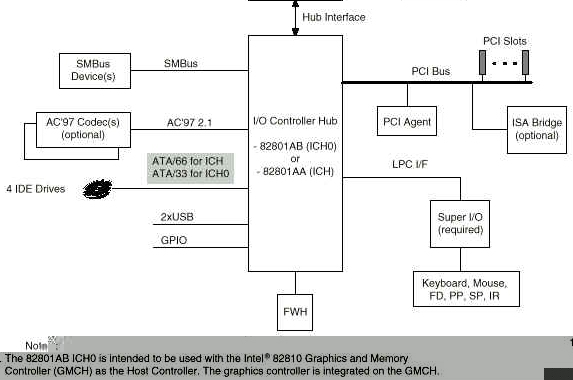
The ICH
This hub, the Input/Output Controller Hub (ICH) is is a highly integrated multifunctional I/O Controller Hub that employs the Intel® Accelerated Hub Architecture (AHA) to make a direct connection from the graphics and memory to the integrated AC97 controller, the IDE controllers, dual USB ports, and PCI add-in cards. The following is the proper break down of components:
PCI Bus Interface, PCI Rev 2.2 compliant ( ICH supports 6 slots and 4 for the ICH0 )
Integrated IDE Controller ( ICH0 supports Ultra ATA/33; ICH supports Ultra ATA/66 )
USB host interface with support for 2 USB ports
AC'97 2.1 Compliant Link for Audio and Telephony CODECs
Power Management Logic ( ACPI 1.0 Compliant, ACPI Power States = S1, S3, S4, S5 )
Low Pin count (LPC) Interface
Enhanced DMA Controller, Interrupt Controller and Timer Functions
Real-Time Clock
System Management Bus (SMBus) compatible with most I2C devices
Supports ISA Bus via External PCI-ISA Bridge
Hub Interface to use AHA
Firmware Hub (FWH) Interface
Alert On LAN Support ( ICH only )
Here again, there are two versions of the ICH, the 82801AA (ICH) and 82801AB (ICH0) hubs. The main differences are that the ICH has support for up to 6-PCI slots, U-ATA/66 and Alert-On-LAN, whereas the ICH0 doesn't have the last features and only has support for 4-PCI slots and U-ATA/33. Here's a graphical view of it:
Besides being Intel's 1st chipset to have integrated video, it is also AC'97 ready. AC'97 ready basically means, external audio and/or telephony codec chips(s) can be fixed on to the motherboard and the chipset refers to these codecs by means of an AC'97 Link and uses CPU power to execute the sound and/or telephony features. Codecs are like written instructions to tell the system how to utilise it, e.g, an Audio-codec tells the system how to run and output audio but all processing is done by the CPU. Now, these codecs are very cheap to include hence, an i810 board essentially can have video, audio and modem functionality, which brings about even cheaper systems based on Intel-Celeron Processors, a market VIA and SIS completely missed to cash-in. We don't have to worry about the CPU utilization as a Celeron can easily spare a few percent of brain-power to give such all-round functionality to a typical Celeron-system (low-mid range home and business users) without taking a big toll in CPU power. After all, isn't this the market where Intel is catering for with this chipset?
But providing the necessary codecs or not, is up to the motherboard manufacturer's choice depending on which audience his motherboard is targeted for. They can even forgo this software method and provide the actual sound or telephony chipsets and integrate it on to the board to produce better sound with almost no performance hit. There is yet one more choice and that is not to provide any of the functions at all and instead use an AMR card that contains the codecs and output connectors and plug into the new AMR-slot which all the i810 boards are equipped with. What is AMR? AMR stands for Audio & Modem Riser card. It does just as what it says, gives Audio and Modem functionality on the cheap. It is similar as to the manufacturer integrating the codecs on the boards except this method doesn't require the codecs to be on board at all, but it's on the AMR card itself. The manufacturer can even combine the two above methods, e.g. provide audio codec on the motherboard but if you need modem ant telephony functions, you can get the appropriate AMR card to handle the functions at a very low cost or get a dedicated PCI-card to handle those functions more effectively. It's really giving more choices for the manufacturer and the user to expand their PC-functionality with different cost, advantage and disadvantages. As of writing this there aren't any commercial AMR cards yet and I guess manufacturers are waiting for the i810 boards to get a bit more popular before going into AMR-card production.
The i810 chipset does not come with an ISA-Bridge Controller by default and is the 1st chipset to omit this but it is an option, which the manufacturer can choose to implement. But since it has now become an option and it is high time for ISA support to be discontinued, most manufacturers will forego the ISA slots.
There is now a new interface called a Low-Pin-Count (LPC) Interface that is used to connect Floppy and other port controllers that used to communicate via the old ISA-bus. Since ISA support is removed from chipset (but can be included by manufacturer at higher cost), the LPC is a 4-bit, 33Mhz bus that is actually a simplified ISA bus.
The Firmware Hub (FWH) Interface is just a small 33Mhz bus to communicate with the FWH where the Bios of both the system and integrated-video are located.
The FWH
If your searching for the big and bulky-looking Bios chip on an i810 board, it won't be there! In it's place is a tiny chip called the Firmware Hub (FWH) which may or may not be socketted (it was socketted on the DFI motherboard). It's size is similar to that of the Bios chips on the new Gigabyte-BX2000 motherboard ( I wonder why it wasn't socketted ). There are 2 versions of the FWH also! The i82802AB is a 4Mbit (512Kb) part and the i82802AC is an 8Mbit part (1Mb!). Currently most motherboards will use the 4Mbit parts, as it's more than enough for typical systems. Now what does tiny hub do? It contains the Bios for both the system and integrated-video. The system Bios has been greatly improved from the Award-Bios that we've been using for ages! Lots more fine-tuned options to choose from for us tweakers. Sorry for the lack of screen-shots in this section. Besides the Bios, it also contains the all-new, Random Number Generator (RNG, which Intel claims it is used for greater security. This is a snippet from the Data-sheets:
"Intel will provide a Windows driver to give third party software access to our RNG for use as a security feature. Also provided will be a device driver developer kit (DDK) for operating system vendors who wish to design security drivers for their platform."
Well, one thing is for sure, that RNG really works! How do I know? When I booted up the PC using the DFI i810 motherboard, during the HDD auto-detection, it will auto-detect your HDD as well as assign a unique number (I didn't take note of how many digits long it was, but it was probably 8 digits). I had 2 HDDs, so 2 very different numbers were assigned to them. When I restated the PC, the numbers change radically for both. I've since re-booted numerous times, never seeing the same pair of numbers again. Why Intel has featured this RNG in hardware is because hardware generated numbers have a far less chance to repeat themselves in a certain given period and the fact that the numbers are bigger than software generated numbers, as claimed by Intel. There are more security related features but if you need to know more and are a bit technical, read-up the Data-sheets. I guess the 8mb version can feature a higher security threshold.
Since we now know how the i810 Architecture works, here's a general pciture of how an i810 boad would look like and location of new components. It's the DFI PW65-D:
Performance
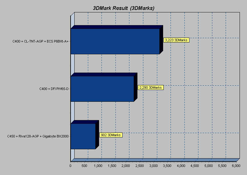
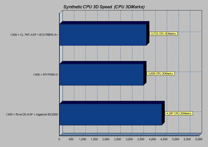
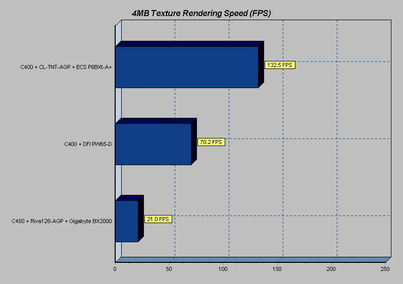
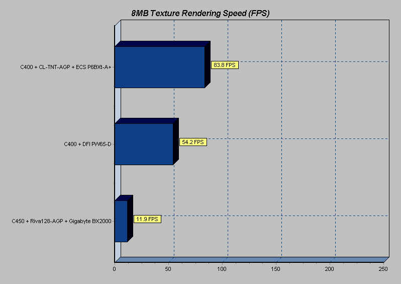
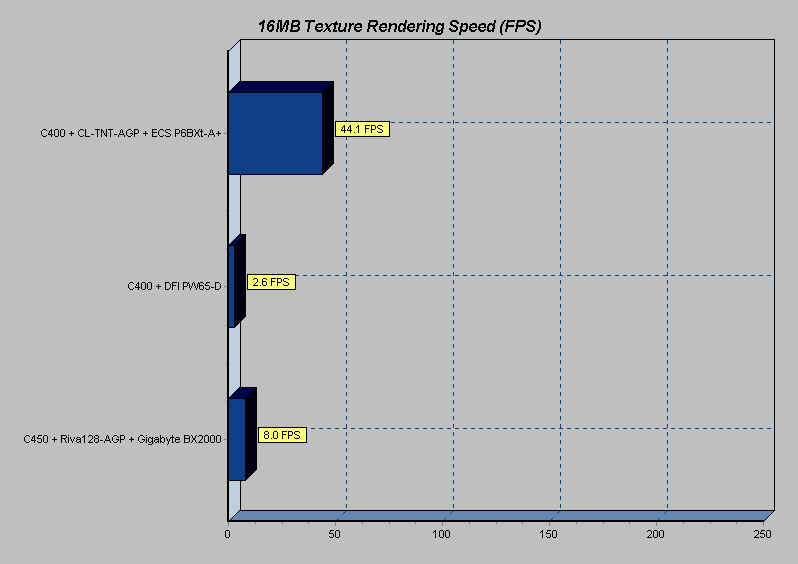
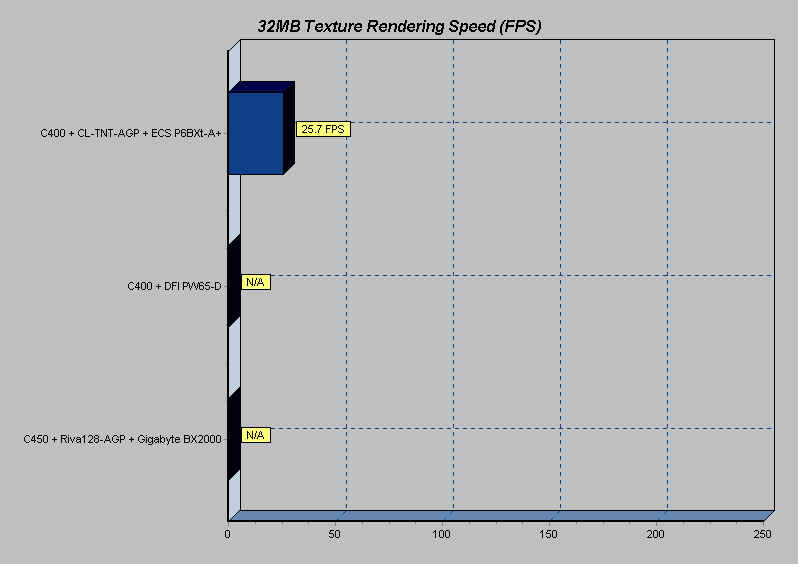
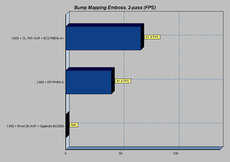
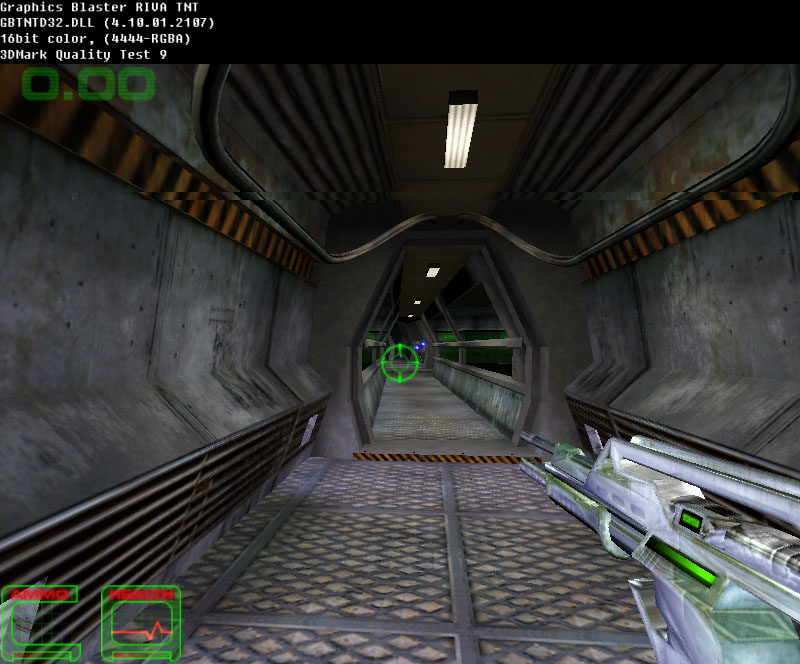
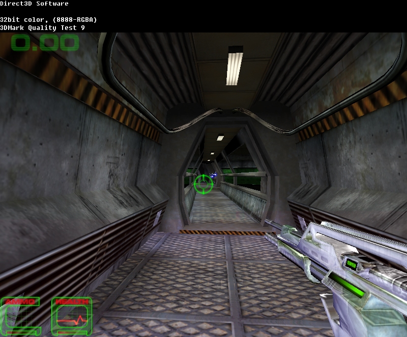
The processor used for this test is a C-300A slot-1 which is of the SL32A batch overclockable to 450 and a C-400 PPGA which is of the SL37X with an Asus Slocket. Since I acquired the C-300A much latter, I can't show many results for it. The C-400 PPGA I had was not overclockable at all even with another MSI Slocket. I will investigate that latter. The column in concern is processor with DFI PW65-D, the Gigabyte BX2000 is a BX-chipset based board for comparison. The Riva-128 video-card was chosen because it is as close as possible to the descendant of the i752 graphics engine that I could test on, the i740 based video cards.
A special thanks to CPU-Zilla who had kindly invited me over to his place to do some of the testing which was not possible with my components. I even found how overclockable my C400 was at his place, up to 500MHz!
Test Configuration
Processor(s): Intel Celeron-400 PPGA SL37X Malay + Asus Slocket &
Intel Celeron-300A Slot-1 SL32A Malay.Motherboards(s): DFI PW65-D
Gigabyte BX2000RAM: 1 - 64MB LGS-7J SDRAM DIMM Hard Drive(s): IBM Deskstar-3 3.2G Video Card(s): Built in i752 graphics engine
Canopus Riva128-AGPBus Master Drivers: Windows 98 Bus Mastering Drivers Video Drivers: 4.11.01.1161 Version PV1.0 Operation System(s): Windows 98 (build 4.10.1998)+ Direct-X 6.1 System Combination(s): DFI PW65-D + built-in i752
Gigabyte BX2000 + Riva128-AGP
ECS P6BX-A + Creative-TNT AGPWintune 98 Results
Area Tested C-400 (66x6)
DFI PW65-DC-400 (66x6)
Gigabyte BX2000CPU Integer (MIPS) 1172.421 1168.128 CPU Floating Point (MFLOPS) 461.7393 460.6635 Video(2D) (MPixeles/s) 65.34016 84.43046 Direct3D (MPixeles/s) 51.48141 100.9557 OpenGL (MPixels/s) 37.82972 70.06438 Memory (MB/s) 666.8571 682.373 Cached Disk (MB/s) 64.7826 70.33907 Uncached Disk (MB/s) 1.785674 1.904453
Other Benchmarks
CPU speed + Motherboard C-400A
(66 x 6)
DFI PW65-DC-400A
(66 x 6)
Gigabyte BX2000ZD CPU-Mark99 29.6 30.3 ZD FPU-WinMark99 2140 2130 ZD Business Winstone99 15.7 15.9 NU Sys Info (pts) 127 116.7 Sisoft CPU benchmark (MIPS) 956 956 Sisoft FPU benchmark (MFLOPS) 271 270 Sisoft memory benchmark (MB/s) 180 182 As you can see, the performance of the board is similar to the BX-chipset motherboard.